The age of the monolithic AI accelerator is over. For years, the industry chased a single chip to rule them all: a magical slab of silicon that could both train gargantuan models and serve them at scale. It was a noble, if naive, quest. The physics of data movement, the emergent demands of “agentic” workflows, and the brutal economics of data center power grids have all conspired to shatter that dream.
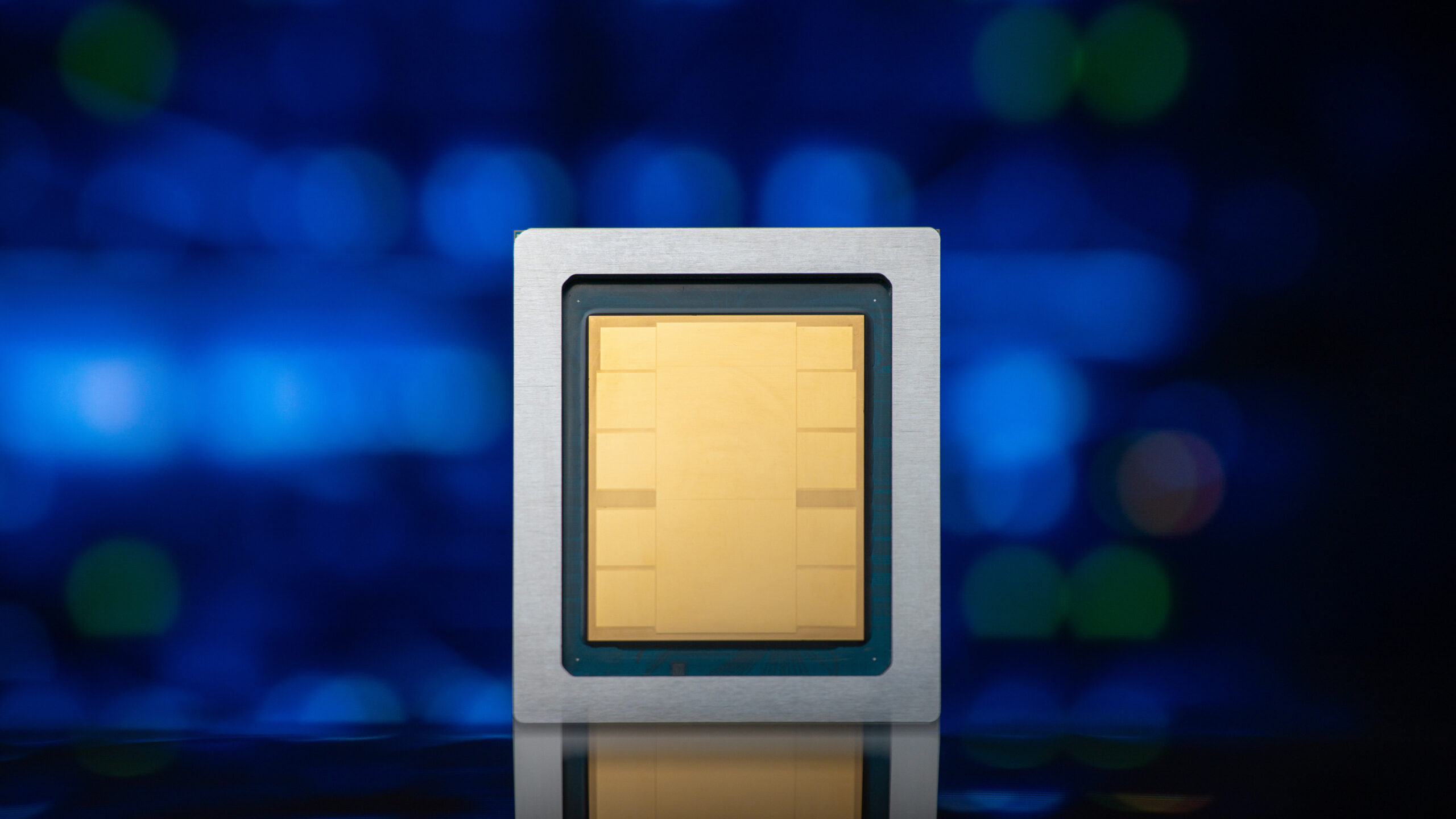
Google’s eighth-generation Tensor Processing Units represent the clearest admission of this new reality. They aren’t a single chip, but a pair: the TPU 8t for training and the TPU 8i for inference. This isn’t a minor tweak, it’s a foundational split that signals a profound shift in how we must think about AI infrastructure. The era of agents, autonomous, reasoning, tool-using models operating in continuous loops, doesn’t just demand more compute. It demands fundamentally different kinds of compute.
Let’s dive into the architecture that makes this possible and what it tells us about the future of scaling AI.
The Physics Problem: Training vs. Inference Are Now Different Sports
Training a frontier model is a marathon run on a superhighway. It’s about moving petabytes of data through thousands of chips with near-perfect synchrony, maximizing aggregate FLOPs over weeks or months. The goal is throughput.
Running inference for swarms of agents is a city-wide relay race with millions of participants. It’s about minimizing latency for individual interactions (“tokens”) while managing massive concurrency. The goal is responsiveness.
Google’s data makes the divergence stark. The TPU 8t superpod scales to 9,600 chips with 2 petabytes of shared high-bandwidth memory and a claimed 121 ExaFlops of compute, designed to collapse model development from months to weeks. Its job is brute force.
The TPU 8i pod, conversely, scales to 1,152 chips but is architected for a different kind of chaos. Its primary innovation isn’t raw FLOPs, but a re-engineered network to prevent a “waiting room” effect. When you have millions of agents, each executing multi-step plans, microsecond delays in chip-to-chip communication cascade into seconds of overall lag. Google’s response includes tripling the on-chip SRAM (to 384 MB) to hold larger KV caches, doubling the Interconnect (ICI) bandwidth to 19.2 Tb/s, and introducing a Collectives Acceleration Engine (CAE) that cuts on-chip collective operation latency by up to 5x.
The takeaway? The hardware spec sheets for training and inference are now written in different languages. One talks in ExaFlops and petabytes, the other in latency, concurrency, and “goodput.”.
The Network Is the Computer, Redefined: Virgo and Boardfly
A cluster of a million chips is useless if they can’t talk efficiently. This is where Google’s most audacious claims live, and they hinge on two new networking topologies.
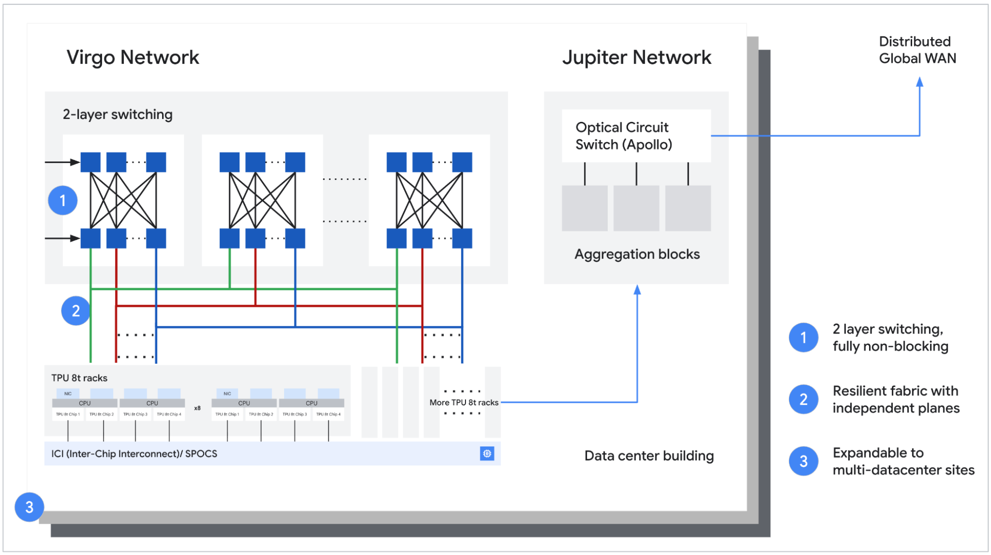
For the TPU 8t training beast, Google unveiled the Virgo Network, a “megascale data center fabric” designed to link over 134,000 chips with up to 47 petabits/sec of non-blocking bisectional bandwidth. Combined with JAX and Pathways software, Google claims this enables near-linear scaling for up to a million chips in a single logical cluster. The goal is to make a data center, or even multiple data centers, behave like one gigantic computer for training runs.
But the 3D Torus topology that works for training’s neighbor-to-neighbor communication patterns becomes a liability for inference. In the agentic world, any chip might need to talk to any other chip instantly to route a token or share state across a swarm.
Enter the Boardfly topology for the TPU 8i. Inspired by high-radix Dragonfly principles, it’s a hierarchical network that drastically reduces the network diameter. In a 1024-chip pod, the maximum hops between any two chips drops from 16 in a 3D Torus to just 7 in Boardfly. This 56% reduction in network diameter is a direct attack on the tail latency that kills agent performance. It’s a topology built not for raw bandwidth, but for all-to-all chatter.
This specialization is expensive. Designing two separate network fabrics is a monumental R&D investment. But it underscores a critical point: generic scaling doesn’t cut it anymore. You need networks designed for the workload, a lesson in distributed compute frameworks like Ray.
The Full-Stack Power Play: Axion, Liquid Cooling, and Goodput
Hardware divergence is only part of the story. Google is leaning into a full-stack co-design philosophy that extends from the silicon to the data center cooling pipes.
A key detail buried in the specs: both TPU 8t and 8i now use Google’s custom Arm-based Axion CPUs as hosts. Previous generations used x86 hosts. By moving to its own silicon for the host CPU, Google eliminates a bottleneck and gains system-level optimization levers x86 vendors can’t provide. It also doubles the physical CPU hosts per server, using a Non-Uniform Memory Architecture (NUMA) for isolation.
Then there’s power. Google claims the new TPUs deliver up to 2x better performance-per-watt over the previous Ironwood generation. In an era where data center power, not chip supply, is the binding constraint, this isn’t a nice-to-have, it’s existential. The integration goes deep: “We integrate network connectivity with compute on the same chip, significantly reducing the power costs of moving data across the TPU pod”, they note. Even the fourth-generation liquid cooling systems are co-designed to sustain performance densities air cooling cannot.
The ultimate metric? Goodput. Google engineers TPU 8t to target over 97% “goodput”, productive compute time versus total uptime. At frontier training scale, they note, every percentage point can translate into days of saved training time. This obsessive focus on usable output, not peak theoretical FLOPS, is what separates infrastructure designed by model-builders from infrastructure designed by chip vendors.
The Agentic Imperative: Why This Split Was Inevitable
All these technical choices circle back to one driver: the rise of autonomous AI agents. As Sundar Pichai noted, the conversation has shifted from “Can we build an agent?” to “How do we manage thousands of them?“
- Long context/state: Larger KV caches must live on-chip (hence 3x SRAM).
- Massive concurrency: Millions of simultaneous sessions require low-latency collective ops (hence the CAE).
- Complex, branching logic: Communication patterns are unpredictable and all-to-all (hence Boardfly topology).
- Continuous learning/reasoning: Blurs the line between training and inference, requiring efficient data movement.
A chip optimized for the steady, predictable, batch-oriented flow of pre-training simply can’t handle this. Trying to force it would be like using a cargo ship for a Uber fleet. The inefficiencies would be catastrophic, blowing up inference costs and compute economics.
The Strategic Implications: Lock-in, Co-design, and the Nvidia Counterpoint
Google’s move is a masterclass in vertical integration and ecosystem lock-in. The TPUs are only available through Google Cloud. The software stack (JAX, Pathways, MaxText) is tuned for this hardware. The Axion CPU host completes the loop. For customers, the performance gains are compelling, up to 2.7x better price-performance for training and 80% better price-performance for inference over Ironwood, according to Google. But adoption means betting your AI future on Google’s stack.
This stands in contrast to the Nvidia + PCIe ecosystem, which offers more vendor flexibility but arguably less holistic optimization. Google’s bet is that the performance delta from full-stack co-design will outweigh the value of choice. For companies embarking on massive infrastructure investment plans
[blog/alibaba-qwen-roadmap-china-ai-scaling-play), this trade-off is the central calculation.
The Bottom Line: Specialization Is the New Scaling Law
The launch of TPU 8t and 8i is more than a product announcement. It’s a thesis on the next decade of AI compute.
The “one chip to rule them all” paradigm is dead, killed by the unique, sprawling demands of agentic AI. Future scaling won’t come from just cramming more transistors onto a monolithic die, but from architectural specialization, dedicated silicon for training, for inference, for memory-bound tasks, for networking.
Google’s dual-TPU strategy is the first major cloud provider to fully and publicly architect for this reality. It sets a benchmark that others must respond to, not just in raw performance, but in the very philosophy of AI infrastructure. The race is no longer just about who has the most chips. It’s about who can most intelligently split them apart.
For practitioners, the message is clear: when evaluating AI infrastructure, stop looking at peak FLOPs. Start asking about network diameter for your specific communication pattern, on-chip SRAM for your expected context length, and the system’s “goodput” under your exact workload. The era of generalized benchmarks is over. The era of workload-specific architecture has begun.
The ultimate success of this architectural gamble won’t be measured in spec sheets, but in its ability to enable a new class of applications. Can it power the simulation of millions of parallel worlds for training world models? Can it orchestrate the real-time, collaborative reasoning of thousands of specialized agents on a single problem? The hardware is now claiming it can. The burden of proof shifts to the software, and the ambitious developers who will use it to redefine what’s possible. In doing so, they’ll force a reckoning on model cost efficiency and benchmarking across the entire industry.