It’s not the compute that’s holding us back anymore. It’s the memory.
While everyone was obsessing over GPU teraflops and parameter counts, the real bottleneck quietly metastasized into what engineers call the “memory wall”, the widening chasm between how fast processors can crunch data and how fast memory can feed it to them. HBM prices nearly doubled during 2026, and the shortage isn’t easing until at least 2028.
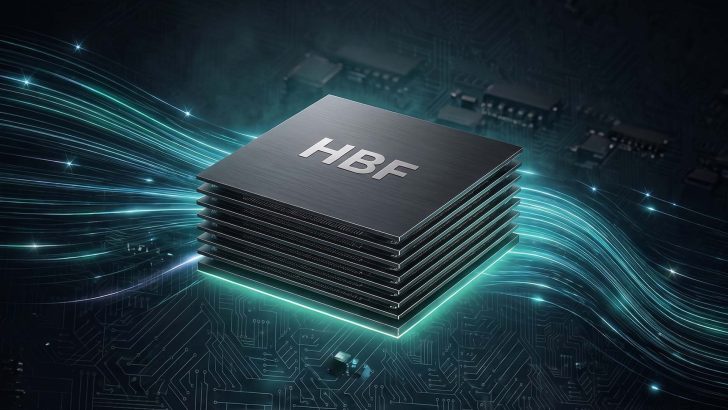
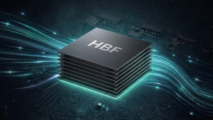
Enter SK hynix and SanDisk with what might be the most consequential memory announcement of the decade: the first open High Bandwidth Flash (HBF) standard, targeting up to 3TB/s of bandwidth and 512GB of capacity per stack. This isn’t just another spec sheet. It’s a fundamental rethinking of where AI models live and how they get fed to your accelerators.
The Unexamined Middle Ground Between HBM and SSDs
Here’s the problem nobody’s been talking about loudly enough: today’s AI memory hierarchy has two speeds, absurdly fast and absurdly slow, with nothing in between.
HBM delivers several TB/s of bandwidth but tops out at tens to low hundreds of gigabytes. Your SSD can hold terabytes, but you’re moving data over PCIe, and the bandwidth is about as exciting as watching paint dry. For AI inference, this forces a brutal trade-off: the model needs to be either small enough to fit in HBM (expensive) or streamed from SSD (slow).
The new HBF standard positions itself as the missing middle gear, a new memory layer between HBM and SSDs that applies HBM-style stacking to NAND flash. The numbers are hard to ignore:
| Memory Type | Bandwidth | Capacity | Best Use |
|---|---|---|---|
| HBM4 | ~2TB/s per stack | Up to 64GB | Data AI chips need immediately |
| HBF | 0.4, 3.0 TB/s | Up to 512GB per stack | Large models kept close to processors |
| Enterprise SSD | ~10-15 GB/s over PCIe | Multiple TB | Long-term storage |
Put bluntly: HBF offers up to 8x the capacity of an HBM4 stack with comparable bandwidth. The most capable HBF implementation at 3TB/s actually beats the bandwidth of a single HBM4 memory stack’s 2TB/s. It won’t win on latency, NAND is never touching DRAM on that metric, but for inference workloads, that might not matter.
Why Inference Is the Perfect Use Case (And Training Isn’t)
The Training Problem
The skeptics will point out, correctly, that NAND flash has higher latency and awful write endurance compared to DRAM. That’s a feature, not a bug, when you think about what inference actually does.
During training, you’re constantly writing gradients and updating weights. Flash would die a miserable, early death. But during inference, your AI system mostly reads model weights instead of continuously rewriting them. This is a workload that plays directly into NAND’s strengths:
Why NAND Wins at Inference
- Read operations don’t wear out flash, write operations do
- NAND’s non-volatility eliminates the constant refresh cycles DRAM requires
- Model weights are static after training, making them ideal for write-once, read-many (WORM) patterns
There’s a reason people are drawing comparisons to Intel’s ill-fated Optane. The sentiment across developer forums is that this approach feels overdue, some are still salty about Intel scrapping that product. But HBF isn’t Optane. It’s a fundamentally different architecture that takes the commodity NAND you already have and reorganizes it for AI workloads.
The math gets interesting with a concrete example. An AI model with 500 billion parameters needs roughly 500GB of storage, assuming each gigabyte can house a billion parameters. It’s not cost-effective to hold that entire model in HBM, you’d need eight HBM4 stacks just for capacity. HBF lets you keep the whole thing one hop away from your compute.
The Technical Specs That Matter
The standard, released through the Open Compute Project (OCP), covers more than just marketing numbers. SK hynix and SanDisk, joined by Google and Tenstorrent in the consortium, defined the whole stack:
- Capacity: Up to 512GB using either 8-high or 16-high NAND die stacks
- Bandwidth grades: Grade 1 through 3, ranging from ~0.4TB/s to 3.0TB/s
- Interface: UCIe (Universal Chiplet Interconnect Express) for connecting across GPU and CPU architectures
- Guidelines: Connection interfaces, electrical characteristics, reliability specs, packaging guidelines, and software I/O requirements
The UCIe adoption is a sleeper hit here. Rather than creating another proprietary interface that locks you into one vendor’s ecosystem, HBF plugs into the existing chiplet interconnect standard. That means it can flexibly integrate with GPUs, CPUs, or whatever new class of AI accelerator emerges, a strategic flex that positions HBF as infrastructure rather than a product.
Interesting wrinkle: SanDisk is describing the interface as “xPU-HBF”, which appears to be their branding of UCIe as implemented by companies like Broadcom or Marvell. The names might differ, but the architecture is designed for heterogeneous computing from day one.
The Computational Ramifications Go Deeper Than You Think
Here’s where this gets genuinely interesting for AI enthusiasts. A 3TB/s bandwidth threshold isn’t just incremental progress. It’s a qualitative shift.
Think about what that means for a GPU with the same memory bandwidth profile as an RTX 5090 (1.75TB/s of VRAM bandwidth). HBF at the top grade exceeds that. If you can stream model weights directly from HBF to the GPU at 3TB/s, the flash stops being the bottleneck.
The speculation happening in engineering circles is that this could enable a new class of accelerator architecture. If you’re feeding weights at 3TB/s directly to a GPU or CPU, you don’t need to move anything into VRAM first. The HBF becomes the working set, and the VRAM becomes just a cache. This could dramatically reduce the cost of running large models by letting you trade expensive HBM capacity for cheaper NAND.
But there’s a practical skepticism worth keeping. The 0.4TB/s baseline grade suggests the first-generation implementations will be closer to 400GB/s than 3TB/s. Extracting that much bandwidth from a single 512GB package requires extremely complex base die silicon, we’re talking about UCIe interfaces running at up to 64 GT/s with 64 lanes. This is specialized hardware, not your run-of-the-mill M.2 SSD.
The Elephant in the Room: Adoption
Here’s the uncomfortable question nobody at the FMS keynote wanted to address directly: who’s actually going to build this?
The HBF consortium currently includes SK hynix, SanDisk, Google, and Tenstorrent. That’s a respectable start, but conspicuously absent are the names that could make or break this standard: Nvidia, AMD, Intel, Micron, Samsung, Qualcomm, and Broadcom. None of them have expressed public interest in HBF.
That’s not necessarily fatal. Open standards have succeeded before with smaller starting coalitions. But it means HBF faces an uphill battle against the inertia of existing memory architectures. Samsung is already developing CMX solutions with Nvidia, targeting the same AI storage bottleneck with V10 and V11 NAND flash that can reach up to 500 stacked layers. The competitive landscape is forming, and it’s becoming clearer that this is now a race, not a monopoly.
The timeline compounds the risk. HBF memory samples aren’t expected until late 2026, with commercial inference devices possibly arriving in early 2027. In AI infrastructure terms, that’s practically a generation away. The AI-driven hardware price surge, which has pushed DRAM contract prices up 55-60% quarter-over-quarter, might ease by then, or it might not.
The Power Efficiency Angle Nobody’s Discussing
Beyond bandwidth, there’s a quieter revolution happening in the same announcement. SK hynix also unveiled its tenth-generation (V10) 375-layer 4D NAND, which delivers 2.5x better performance per watt than the previous generation.
That’s not just a spec sheet bragging point. It’s an infrastructure-level advantage. Data centers are increasingly power-constrained, not by floor space, not by cooling, but by electricity itself. If HBF can serve model weights at acceptable bandwidth while consuming a fraction of the power HBM demands, it changes the economics of AI inference deployment.
Here’s the causal chain: NAND doesn’t need constant refresh. During inference, an HBF device sits mostly idle, drawing minimal power until it needs to stream weights. An HBM stack, by contrast, is always-on, always-refreshing, always burning power even when you’re only using a fraction of its capacity.
For inference workloads, which represent the bulk of AI compute in production, that power profile is arguably more important than raw bandwidth.
What This Means for Local AI (And Your Wallet)
The realistic take for individual developers and enthusiasts is more measured than the hype suggests. The first HBF implementations will almost certainly be data center-only, and the 80-160B model gap that plagues local hardware won’t vanish overnight.
But here’s the longer play: if HBF succeeds in the data center, it pulls down the cost of serving large models significantly. That reduces the cost of API access, which benefits everyone. It also creates a pathway for the technology to trickle down to workstations and eventually consumer hardware, though that’s likely years away.
There’s also the infrastructure ripple effect. High-bandwidth memory has become so expensive that enterprise RAM prices have surpassed consumer GPUs on a per-gigabyte basis. Standards like HBF that offer a cheaper, power-efficient alternative to HBM create competitive pressure that could eventually moderate memory pricing across the board.
HBF isn’t a revolution in the sense of replacing HBM. It’s a revolution in the sense of finally giving AI architects a third option.
The current binary choice, expensive but fast HBM, or cheap but slow SSDs, has constrained how AI systems get built. HBF’s promise of NAND-level economies with HBM-adjacent bandwidth could enable architectures that simply weren’t possible before. Models that couldn’t fit in HBM without bankrupting you can now live one hop from compute.
The standard is open, the consortium is growing, and the technical specifications are genuinely compelling. Whether the rest of the industry gets on board, particularly the GPU vendors who would need to support UCIe-connected HBF, remains the critical variable that will determine whether this is a footnote in memory history or a foundational shift in AI infrastructure.
The memory wall just got a ladder. Whether anyone climbs it is a different question entirely.