The Tesla V100 is a piece of hardware that, in official channels, still commands a premium. It’s the GPU that powered the first wave of modern AI breakthroughs, and NVIDIA has long since moved on to the H100 and beyond. But for the global community of hackers, tinkerers, and budget-conscious AI startups, the V100 remains a coveted workhorse. The only problem? Getting your hands on one that isn’t a salvage pull from a decommissioned server cluster, and making it play nice with friends via NVLink, has been a nightmare.
That just changed. A team of hackers in China, one reportedly a graduate of Tsinghua University, has done what many assumed was impossible: they fully reverse-engineered the Tesla V100’s 2,963 pinout signals and fabricated a brand-new, custom half-height PCB. They call it the “Tesla V100 v4.” More importantly, they’ve made it work with NVLink, up to an 8-way configuration.
The pricing is the real headline. The 16GB version clocks in at 1,499 RMB ($220 USD), and the 32GB version hits 3,999 RMB ($590 USD). A 2-way NVLink adapter is a mere $29, while an 8-way NVLink bridge is $118. For context, a single, officially used 32GB V100 on eBay still hovers around $1,500-$2,000. The hackers are offering a “new” one, with a 3-year warranty, for a third of the price. This isn’t just a discount, it’s a paradigm shift in how we think about access to enterprise-grade compute.

The Guts: A Year of Pin-Sniffing and a Half-Height Miracle
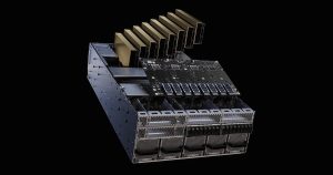
Let’s talk about what this actually took. The Tesla V100 uses the SXM2 form factor. This isn’t a standard PCIe card you can just plug into your motherboard. It requires a proprietary backplane to handle power delivery and the complex routing of NVLink, NVIDIA’s high-speed interconnect. Sourcing that backplane was already a niche hell.
The hacker team didn’t just buy a backplane. They literally traced every single one of the 2,963 pins on the GPU package. They mapped each signal, ground, power, data lane, clock, and figured out the proprietary routing required to make it all talk to a PCIe host and other GPUs. The result is a PCB that is smaller than the original SXM2 module, fitting into a half-height slot. This has massive implications for dense, cluster-style deployments. You can now fit more compute into less space, assuming you can solve the thermal challenge.
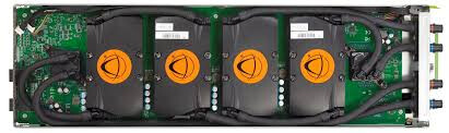
The NVLink implementation is the hardest part. NVLink isn’t just a faster PCIe lane, it’s a complex mesh fabric protocol. To get 8-way communication, you historically needed NVSwitch ASICs. The community initially dismissed the 8-way claims, with one developer stating, “8 way NVLINK needs NvSwitch which required 4 ASICs for handling the switching, so it not gonna happens.” But the team appears to have overcome this, and the resultant adapter board is reportedly scheduled for a July shipment.
More Than a Clone: A New Ecosystem
This isn’t just a one-off hack. The ecosystem around this is growing fast. The same team is developing NVLink adapter cards that connect via MCIO connectors to your computer, offering 100GB/s of bandwidth between GPUs. This effectively turns a cluster of these cards into a unified pool of HBM2 memory.
There is a palpable demand for this level of integration. One user on the Level1Techs forums is actively trying to design an open-source backplane for 4x V100 SXM2 modules, hoping to create a solution people can build themselves. The Fujitsu CX400M4 boards are often cited as the ideal reference design, but they are expensive and hard to find. The Chinese hackers are, in effect, creating the consumer-grade version of that enterprise hardware.
The Hot Take: The Engineering Is Impressive, But the IP Questions Are Burning
The technical achievement is undeniable. But the legal status is a minefield. While the core GPU die is still NVIDIA’s IP, the PCB layout, the signal routing, and the NVLink adapter are new creations. On Reddit, a cynic asked, “I wonder do they really reverse engineered or Schematic fell off the truck”, pointing out that the V100 SXM PCB file is, in fact, available online. Whether the team spent a year “decoding” a PDF or running expensive X-ray scans on an existing board is unclear. But the act of fabrication and the creation of a new, competitive product is a direct challenge to NVIDIA’s hardware business model.
This taps into a much larger, emerging trend. US sanctions and export controls on high-end AI hardware are forcing Chinese AI labs to get creative. While the V100 is not under a direct embargo, the ability to clone and produce it cheaply signals a degradation of NVIDIA’s pricing power in the secondary market. This is one of the primary mechanisms by which how US sanctions paradoxically accelerated Chinese AI capabilities.
What This Means for the AI Hardware Market
For a startup trying to fine-tune a 7B parameter model or run a small inference server, this is a revolution. You could build an 8-GPU, 256GB HBM cluster for under $5,000. That hardware would be competitive for a massive range of AI workloads, from Llama-3-70B inference to stable diffusion ensembles. The economics of this change everything.
| Configuration | Cost (Hacker Board) | Estimated Cost (Official eBay) | Savings |
|---|---|---|---|
| Single 16GB V100 | $220 | $800 | 72% |
| Single 32GB V100 | $590 | $1,800 | 67% |
| 4x 32GB with 8-way NVLink | $2,360 | $7,200 | 67% |
| 8x 32GB with 8-way NVLink | $4,720 | $14,400 | 67% |
It also puts immense pressure on the datacenter. If you can run a comparable workload for a fraction of the cost, the argument for buying a brand-new Blackwell GPU gets a lot harder to make. NVIDIA’s lock-in for AI training was always about the software (CUDA) and the networking (NVLink/NVSwitch). The hardware clones are attacking the hardware cost.
The Final Verdict: A Slap in the Face to the Status Quo
There are valid concerns about reliability, driver compatibility, and the longevity of these custom boards. A V100 is a 300W compute beast, and the passive cooling solution on a half-height card looks borderline impossible without serious airflow. The team offers a water cooling kit, which suggests they know the limitation.
Despite those caveats, this is the most significant piece of hardware reverse engineering in the PC space in years. It shows that the gap between “datacenter tech” and “garage hacking” is shrinking. It shows that the knowledge required to build these systems is becoming more common.
For the AI community, this is a win for accessibility. For NVIDIA’s legal team, it’s a headache. For the rest of us watching, it’s just a hell of a good story about a team that wanted cheap compute and decided to build their own. The implications for security are also profound, as Chinese state-sponsored hackers leverage available hardware and software tools to push the envelope of what’s possible outside of official supply chains. The era of affordable, cluster-ready AI compute is here, and it arrived via a Bilibili video and a ridiculous amount of autism.